Educational Resources
This page contains some useful information to those studying or researching optical process in semiconductors, especially in the context of optoelectronics. It starts with an overview aimed at a general audience to get an idea of the science related to my research. Further down the page contains more technical content, intended to be a bridge between textbook fundamental science and research of next generation materials. I will aim update this page over time.
Photoluminescence
What is photoluminescence?
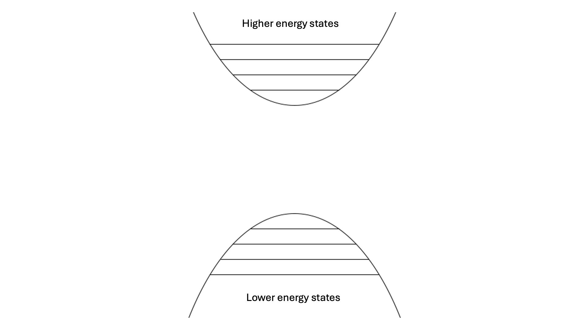
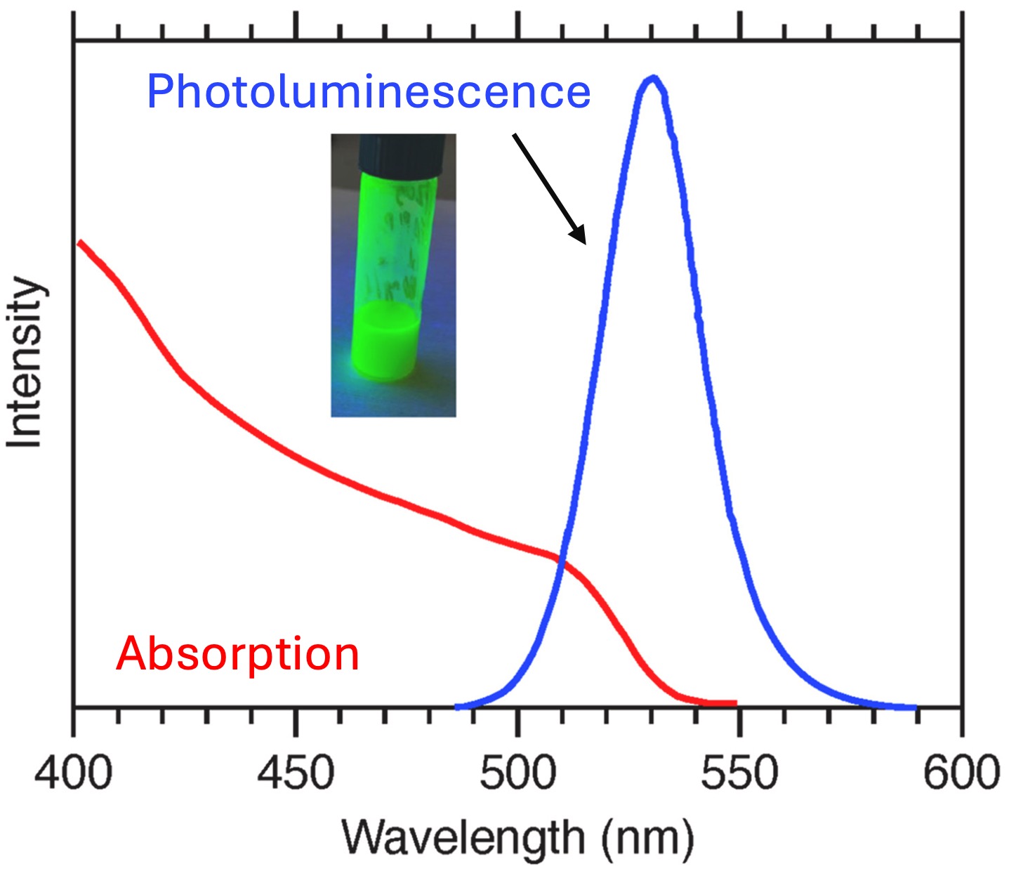
When light is absorbed by a material, the energy must go somewhere. One possibility is that the energy is released in the form of light once again, following the exact reverse process of light absorption. We call this process photoluminescence, referring to luminescence (emission of light), following the process of light absorption.
Shown on the right, the energy of an absorbed photon is first transferred to an electrical charge (electron). The electron returns to the lower energy state over time, releasing energy as a photon. Due to a small amount of energy lost as heat, the emitted photon may have a different energy (colour or wavelength) than the absorbed photon. We can measure the energy of the photons emitted and obtain a photoluminescence spectrum or measure the time taken for the emission of a photon to obtain the photoluminescence lifetime.
What makes photoluminescence so interesting or useful?
Photoluminescence experiments can tell us a lot of information about processes occurring in a material following the absorption of light. This is important for materials used in energy conversion (such as solar cells) or light emission. These are often semiconductor materials, used in many technologies. Measuring the photoluminescence spectrum can tell us about their fundamental properties and potential defects. Measuring the duration of photoluminescence events can tell us how long free electrons survive following light absorption, which is key if we want enough time extract them to use for electrical power.
Excitons
In materials such as semiconductors, when an electron gains energy following absorption of light, it leaves behind a gap which is positively charged. Since positive and negative charges attract each other, they may become bound as a quasiparticle known as an exciton. Excitons are commonly observed in nanomaterials since electrons are strongly confined.
Excitons have a lower energy than free negative (electrons) and positive (holes) charges. The difference in energy is known as the exciton binding energy, which can be ascertained from absorption and photoluminescence spectroscopy. This value determines whether excitons or free charges are formed following the absorption of light.
Magneto-photoluminescence
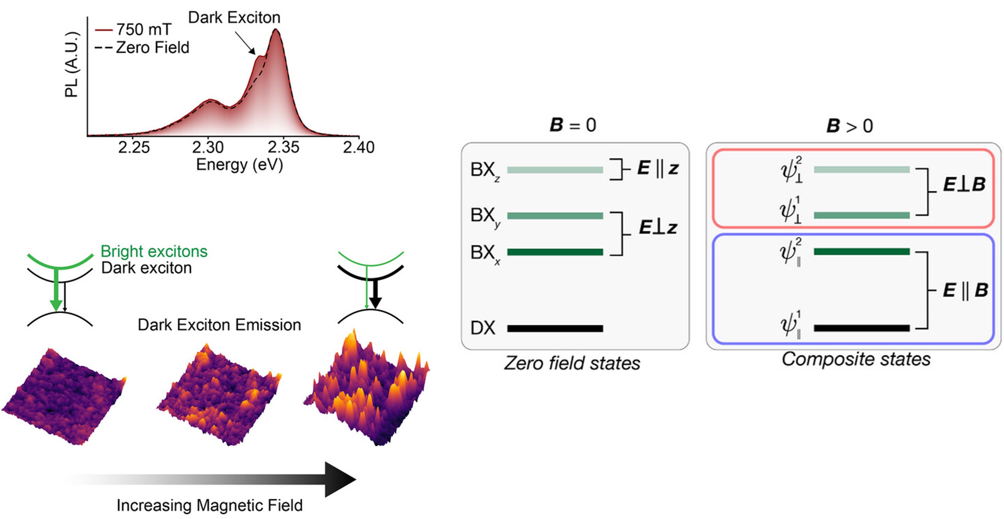
If we record a photoluminescence spectrum from a material while applying an external magnetic field, we may see a difference which gives us further information about the energy states of electrons or excitons. An example of this magneto-photoluminescence of exciton emission in 2D perovskite materials is shown where the light emitted changes colour under a magnetic field. By looking at magneto-photoluminescence under a microscope, we can reveal different localised populations of excitons in the material.
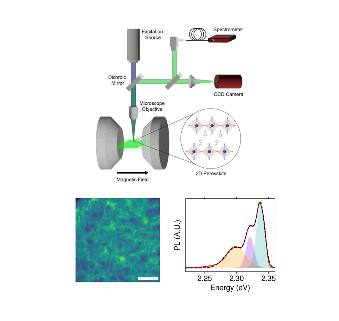
Read the section below on ‘bright and dark excitons’ for further details.
Bright and Dark Excitons
Some materials have exciton states which can absorb and emit light, while also having other exciton states where these processes are forbidden according to optical selection rules. We refer to the former as ‘bright’ excitons and the latter as ‘dark’ excitons. The selection rules are often related to conservation of spin or momentum. This is important for optoelectronic applications, since dark excitons can inhibit the absorption and emission of light.
Excitons in 2D perovskites
In 2D perovskites such as (PEA)$_2$PbI$_4$ there are three bright excitons, each with total angular momentum of one ($J=1$), and one dark exciton with $J=0$. We can identify bright and dark exciton states by using magneto-optical spectroscopy, such as magneto-photoluminescence (described above).
Under a magnetic field, $B$, in the Voigt geometry, the four zero-field exciton states $\vert BX_x\rangle$, $\vert BX_y\rangle$, $\vert BX_z\rangle$ (bright excitons), and $\vert DX\rangle$ (dark exciton) for (PEA)$_2$PbI$_4$ are mixed to form four new states, which can be represented by,
$\vert\psi_\parallel^1\rangle = c_1 \vert DX\rangle + d_1(\vert BX_x\rangle - \vert BX_y\rangle) \tag{1}$
$\vert\psi_\parallel^2\rangle = c_2 \vert DX\rangle + d_2(\vert BX_x\rangle - \vert BX_y\rangle) \tag{2}$
$\vert\psi_\perp^1\rangle = c_3 \vert BX_z\rangle + d_3(\vert BX_x\rangle + \vert BX_y\rangle) \tag{3}$
$\vert\psi_\perp^2\rangle = c_4 \vert BX_z\rangle + d_4(\vert BX_x\rangle + \vert BX_y\rangle) \tag{4}$
Here, the coefficients $c_i$ and $d_i$ are magnetic field-dependent and are functions of the field strength, exciton splitting energies, and exciton $g$-factors. The eigenstates $\vert\psi_\parallel^1\rangle$ and $\vert\psi_\parallel^2\rangle$ have dipole moments (and therefore electric field, $\boldsymbol{E}$, of coupled light) aligned parallel to the magnetic field ($\boldsymbol{E} \parallel \boldsymbol{B}$), while $\vert\psi_\perp^1\rangle$ and $\vert\psi_\perp^2\rangle$ possess dipole moments oriented perpendicular to the magnetic field ($\boldsymbol{E} \perp \boldsymbol{B}$). Since $\vert\psi_\parallel^1\rangle$ and $\vert\psi_\parallel^2\rangle$ are a mixture of the zero-field bright and dark exciton states, an applied magnetic field essentially redistributes oscillator strength between the dark exciton state ($\vert DX\rangle$) and the bright in-plane states ($\vert BX_{x,y}\rangle$).
The effect we observe is a brightening of the zero-field dark exciton state and a darkening of the bright exciton state photoluminescence.
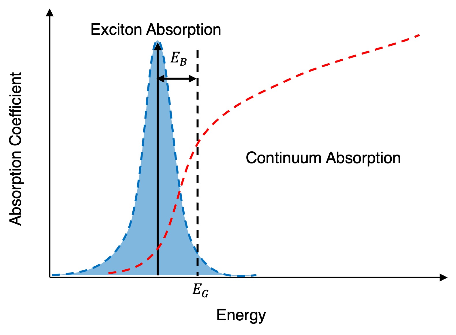
Elliott’s theory for optical absorption
If we obtain an optical absorption spectrum of a material, we can model it using Elliott’s’ theory to obtain an estimate of useful material properties such as the exciton binding energy and bandgap. The model accounts for both exciton and free carrier absorption, with the absorption coefficient given by,
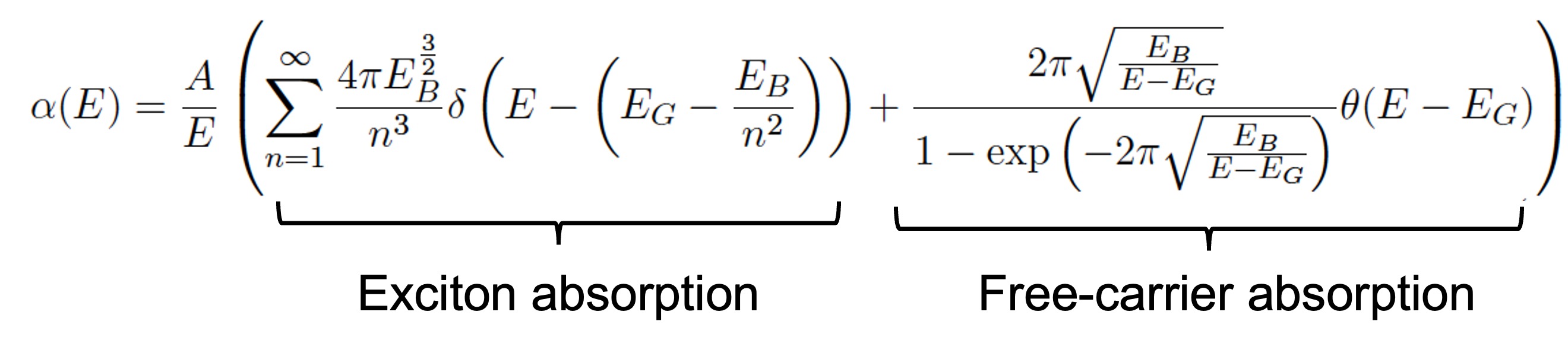
where $E$ is the photon energy, $A$ is a scaling factor that accounts for the transition dipole moment $\langle\psi_v|qr|\psi_c\rangle^2$, $E_B$ is the exciton binding energy and $E_G$ is the bandgap energy. The theory encompasses the contribution of absorption of photons by both exciton states within the bandgap, and also via band-to-band transitions. The former is characterised by a series of delta functions due to the discrete nature of exciton transitions. The band-to-band (free-carrier) absorption is described by a step function, proportional the square root of the photon energy for all real values of $\sqrt{(E - E_G)}$ and zero elsewhere. This function represents the joint density of states in a direct bandgap semiconductor.